Product overview
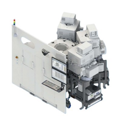
Nice-Tech MC150/MC200/MC300 series MOCVD equipment adopts the close-coupled vertical showerhead gas injection model, with inherent epitaxial uniformity advantages via high-density staggered source gas nozzles and controllable small injection distance. The three models are designed with differentiated reaction chamber sizes for gradient production capacity, supporting flexible substrate configuration and customized design. The whole machine has passed SEMI-S2 and SEMI-S6 certification, with MO source gas circuits up to 10 paths and Hyd gas circuits up to 6 paths, suitable for the growth of 2nd to 4th generation semiconductors and two-dimensional materials, covering R&D, pilot test and mass production scenarios.
Advantages
1. Superior Epitaxial Performance: Ga₂O₃ epitaxial layer on-wafer thickness std 0.19%, InP/GaAs-based materials with low background concentration and high PL wavelength uniformity; excellent crystal quality with step-flow growth of epitaxial surface.
2. Wide Material Adaptability: Full coverage of 2nd to 4th generation semiconductors and two-dimensional materials, one device meeting multiple growth needs.
3. Flexible & Customizable: Gradient substrate configuration, upgradeable gas circuits/thermostatic baths, optional in-situ monitoring functions, supporting personalized customization.
4. High Safety & Easy Operation: SEMI-S2/SEMI-S6 certified; humanized design for simple operation and maintenance, reasonable layout of maintenance area.
5. Stable Process System: Exclusive gas circuit and thermostatic bath configuration for different materials, high-precision MFC/PC control, ensuring stable and accurate growth process.
Applications
Semiconductor Material Growth: Capable of growing 2nd generation (AlGaInAs, AlGaInP, InGaAsP), 3rd generation (GaN, InGaN, AlN), 4th generation (Ga₂O₃) semiconductors and two-dimensional materials (graphene, MoS₂, WSe₂).
Terminal Fields: Applied to prepare thin film materials for power devices, solar cells, VCSEL, lighting, display and optical communication, and used in new energy vehicles, 5G base stations, photovoltaic/wind power generation, radar and satellite communication, etc.
Scenario Matching: MC150 for laboratory R&D, MC200 for medium-batch production, MC300 for large-scale industrial mass production.
Parameters
|
Index |
MC150 |
MC200 |
MC300 |
|
Maintenance Area Size (mm) |
6200*2900 |
7680*3900 |
7680*3900 |
|
Substrate Size Configuration |
6x2", 1x4", 1x6" |
12x2", 3x4", 1x6", 1x8" |
19x2", 5x4", 3x6", 1x8", 1x12" |
|
Core Safety Certification |
SEMI-S2, SEMI-S6 |
||
|
Max MO Source Gas Circuits |
10 paths |
||
|
Max Hyd Gas Circuits |
6 paths |
||
|
Max Thermostatic Baths |
/ |
6 large or 8 small |
6 large or 8 small |
|
Standard Monitoring Function |
Reflectivity/temperature in-situ monitoring (R/T) |
||
|
Optional Core Functions |
Ceiling function, adjustable Process Gap (5~25mm), warpage in-situ monitoring (C), MO source concentration on-line monitoring |
||
|
Typical Process Performance (Ga₂O₃) |
On-wafer thickness std 0.19%; 500nm thick β-Ga₂O₃ surface RMS 0.254nm |
||
|
Typical Process Performance (InP/GaAs-based) |
PL wavelength distribution std as low as 0.014%; low background concentration, high mobility |
||
|
Applicable Scenario |
Laboratory R&D, small-batch pilot test |
Medium-batch production, industrial pilot test |
Large-scale industrial mass production |
|
Gas Circuit Control |
High-precision MFC/PC for all gas circuits |
||
FAQ
Q: What materials can the equipment grow?
A: 2nd/3rd/4th-gen semiconductors (AlGaInAs, GaN, Ga₂O₃, etc.) and 2D materials (graphene, MoS₂, WSe₂).
Q: What safety certifications does it have?
A: SEMI-S2, SEMI-S6 certified.
Q: Can the gas/temperature system be upgraded?
A: Yes. Max 10 MO gas paths, 6 Hyd gas paths; MC200/300 can hold up to 6 large/8 small thermostatic baths.
Q: What monitoring functions are available?
A: Standard: R/T in-situ monitoring; Optional: warpage monitoring, adjustable Process Gap, MO concentration online monitoring.
Q: Key process performance highlights?
A: Ga₂O₃: on-wafer thickness std 0.19%, surface RMS 0.254nm (500nm); InP/GaAs: PL std 0.014%, low background concentration.
Q: Is customized design supported?
A: Yes, customized substrate, gas/temperature modules and monitoring functions are available.
Hot Tags: standard mocvd system, China standard mocvd system manufacturers, suppliers, LPCVD System, LPCVD Furnace, thin film deposition equipment, 3D Surface Topography Measurement System, 3D Optical Surface Measurement System, Low Pressure Chemical Vapor Deposition Equipment