

Low-Pressure Chemical Vapor Deposition (LPCVD) equipment has long been a cornerstone in the semiconductor and thin - film industries. As a supplier of LPCVD equipment, I am often asked about its suitability for research and development (R&D) purposes. In this blog, we will explore the capabilities of LPCVD equipment in R&D, comparing it with other related technologies, and highlighting its unique advantages.
Understanding LPCVD Technology
LPCVD is a process that deposits thin films on substrates at low pressures, typically in the range of 0.1 to 10 Torr. The low pressure environment allows for better control over the deposition rate and film quality. During the LPCVD process, precursor gases are introduced into a reaction chamber where they react at elevated temperatures on the substrate surface, forming a thin film. This process is widely used for depositing materials such as silicon nitride, polysilicon, and silicon dioxide, which are crucial in semiconductor devices, microelectromechanical systems (MEMS), and optoelectronic devices.
Advantages of LPCVD Equipment for R&D
Precision and Control
One of the key advantages of LPCVD equipment for R&D is its high level of precision and control. The low pressure environment enables researchers to accurately control the deposition rate, film thickness, and composition. This is essential for R&D projects where the properties of the thin film need to be carefully tuned. For example, in the development of new semiconductor devices, the thickness and composition of the gate oxide layer can significantly affect the device's performance. With LPCVD equipment, researchers can precisely control these parameters, leading to more reliable and reproducible results.
Uniformity
LPCVD equipment can achieve excellent film uniformity across large substrates. This is important for R&D applications where the performance of the thin film needs to be consistent over a large area. For instance, in the production of solar cells, a uniform thin - film coating can improve the overall efficiency of the cell. The ability to deposit uniform films allows researchers to study the properties of the thin film without being affected by variations in thickness or composition.
Compatibility with Various Materials
LPCVD equipment is compatible with a wide range of precursor gases, which means it can be used to deposit different types of thin films. This versatility is highly beneficial for R&D, as researchers can explore new materials and combinations. For example, they can study the properties of different silicon - based materials or experiment with new compound semiconductors. The ability to work with multiple materials expands the scope of R&D projects and opens up new possibilities for innovation.
Comparing LPCVD with Other CVD Technologies
MOCVD
MOCVD (Metal - Organic Chemical Vapor Deposition) is another popular CVD technology. While MOCVD is often used for the growth of compound semiconductors such as GaN, InP, and GaAs, LPCVD is more commonly used for depositing silicon - based materials. MOCVD typically operates at higher pressures and uses metal - organic precursors, which can be more expensive and require more complex handling. In contrast, LPCVD uses simpler precursor gases and operates at lower pressures, making it more cost - effective and easier to operate for certain R&D projects.
PECVD
PECVD (Plasma - Enhanced Chemical Vapor Deposition) uses plasma to enhance the chemical reactions during the deposition process. This allows for lower deposition temperatures, which can be beneficial for some heat - sensitive substrates. However, the plasma can also introduce defects in the thin film. LPCVD, on the other hand, operates at higher temperatures but does not rely on plasma, resulting in fewer defects and better film quality in many cases. For R&D projects where high - quality films are required, LPCVD may be a more suitable choice.
Applications of LPCVD Equipment in R&D
Semiconductor Device Research
In semiconductor device research, LPCVD equipment is used to deposit thin films for various purposes. For example, it can be used to deposit the gate dielectric layer in MOSFETs (Metal - Oxide - Semiconductor Field - Effect Transistors). By precisely controlling the thickness and composition of the gate dielectric, researchers can improve the device's performance, such as reducing leakage current and increasing the drive current. LPCVD can also be used to deposit polysilicon layers for interconnects and resistors in integrated circuits.
MEMS Research
MEMS devices often require thin films with specific mechanical and electrical properties. LPCVD equipment can be used to deposit silicon nitride and polysilicon films, which are commonly used in MEMS structures. For example, silicon nitride films can be used as insulating layers or as structural materials in micro - cantilevers. The ability to control the stress and thickness of these films is crucial for the proper functioning of MEMS devices.
Optoelectronic Device Research
In optoelectronic device research, LPCVD can be used to deposit thin films for waveguides, optical filters, and anti - reflection coatings. The high - quality and uniform films deposited by LPCVD can improve the optical performance of these devices. For example, a uniform anti - reflection coating can reduce the reflection of light from the surface of an optical device, increasing its efficiency.
Our LPCVD Equipment for R&D
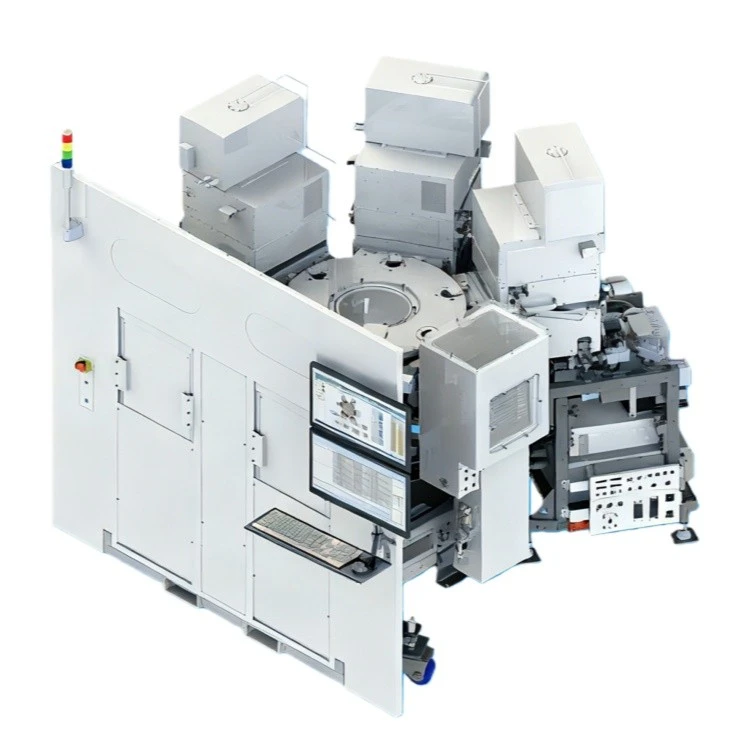
As a supplier of LPCVD equipment, we offer a range of products that are specifically designed for R&D purposes. Our Vertical LPCVD System provides excellent temperature control and gas distribution, ensuring high - quality film deposition. The system is also highly flexible, allowing researchers to easily adjust the process parameters to meet their specific requirements.
We also provide comprehensive technical support and training to our customers. Our team of experts can assist researchers in setting up the equipment, optimizing the deposition process, and troubleshooting any issues that may arise. This support is crucial for R&D projects, as it allows researchers to focus on their research rather than dealing with equipment - related problems.
Conclusion
In conclusion, LPCVD equipment is well - suited for research and development purposes. Its precision, control, uniformity, and compatibility with various materials make it a valuable tool for researchers in the semiconductor, MEMS, and optoelectronic industries. While other CVD technologies such as MOCVD and PECVD have their own advantages, LPCVD offers unique benefits that are particularly useful for R&D.

If you are involved in R&D projects and are interested in using LPCVD equipment, we encourage you to contact us for a detailed discussion. Our team is ready to help you find the most suitable equipment for your specific needs and provide you with the support you need to achieve your research goals.
References
- Sze, S. M. (1985). VLSI Technology. McGraw - Hill.
- Madou, M. J. (2002). Fundamentals of Microfabrication: The Science of Miniaturization. CRC Press.
- Deal, B. E., & Grove, A. S. (1965). General relationship for the thermal oxidation of silicon. Journal of Applied Physics, 36(12), 3770 - 3778.


