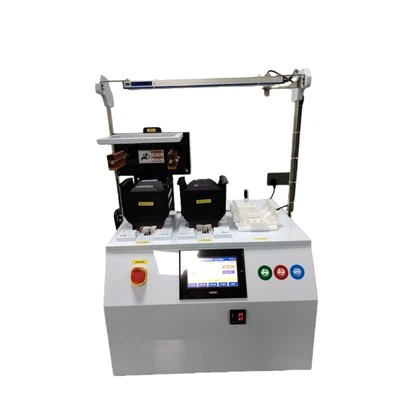
The electrical conductivity of a TC Wafer is a crucial property that significantly impacts its performance and applications in various industries. As a leading supplier of TC Wafer, I am excited to delve into the details of this important characteristic.
Understanding Electrical Conductivity
Electrical conductivity is a measure of a material's ability to conduct an electric current. It is the reciprocal of electrical resistivity and is typically denoted by the Greek letter sigma (σ). The SI unit of electrical conductivity is siemens per meter (S/m). A material with high electrical conductivity allows electrons to move freely through it, while a material with low conductivity restricts the flow of electrons.
Factors Affecting the Electrical Conductivity of TC Wafer
Several factors influence the electrical conductivity of a TC Wafer. These include:
Material Composition
The composition of the TC Wafer plays a fundamental role in determining its electrical conductivity. TC Wafers are often made from specific semiconductor materials, and the type and concentration of dopants added to these materials can significantly alter their conductivity. Dopants are impurities intentionally introduced into the semiconductor to change its electrical properties. For example, adding a small amount of a Group III element (such as boron) to a silicon-based TC Wafer creates a p-type semiconductor, which has a different conductivity profile compared to an n-type semiconductor created by adding a Group V element (such as phosphorus).
Crystal Structure
The crystal structure of the TC Wafer also affects its electrical conductivity. A well - ordered crystal lattice allows electrons to move more freely, resulting in higher conductivity. Defects in the crystal structure, such as dislocations, vacancies, or impurities, can scatter electrons and reduce the conductivity. During the manufacturing process of TC Wafers, techniques are employed to minimize these defects and ensure a high - quality crystal structure.
Temperature
Temperature has a significant impact on the electrical conductivity of TC Wafers. In general, for semiconductors like those used in TC Wafers, the conductivity increases with increasing temperature. This is because at higher temperatures, more electrons are excited from the valence band to the conduction band, increasing the number of charge carriers available for conduction. However, at extremely high temperatures, the increased thermal vibrations of the atoms in the lattice can also scatter electrons, which may start to limit the conductivity increase.
External Fields
External electric and magnetic fields can also affect the electrical conductivity of TC Wafers. An applied electric field can accelerate the movement of charge carriers, increasing the current flow. A magnetic field can cause the charge carriers to move in curved paths, which can change the effective conductivity of the material. These effects are often utilized in various semiconductor devices based on TC Wafers.
Measuring the Electrical Conductivity of TC Wafer
There are several methods for measuring the electrical conductivity of TC Wafers. One common method is the four - point probe technique. In this method, four equally spaced probes are placed on the surface of the TC Wafer. A current is passed through the outer two probes, and the voltage is measured across the inner two probes. Using Ohm's law and the known geometry of the probes, the resistivity of the wafer can be calculated, and then the conductivity can be obtained as its reciprocal.
Another method is the van der Pauw method, which is suitable for measuring the conductivity of samples with arbitrary shapes. In this method, four contacts are placed at the edges of the TC Wafer, and different current - voltage configurations are used to calculate the resistivity and conductivity.
Applications Based on Electrical Conductivity
The electrical conductivity of TC Wafers makes them suitable for a wide range of applications:
Integrated Circuits
In the field of integrated circuits, TC Wafers are used as the base material. The controlled electrical conductivity allows for the creation of transistors, diodes, and other electronic components on the wafer. By carefully doping different regions of the wafer, it is possible to create complex circuits with specific electrical properties.
Sensors
TC Wafers can be used to fabricate sensors that rely on changes in electrical conductivity. For example, gas sensors can be designed such that the presence of a particular gas changes the conductivity of a thin film on the TC Wafer. This change in conductivity can be measured and used to detect the gas concentration.
Solar Cells
In solar cells, the electrical conductivity of TC Wafers is crucial for converting sunlight into electricity. The semiconducting properties of the wafer allow for the generation of electron - hole pairs when exposed to sunlight. The conductivity of the wafer enables the efficient collection and transport of these charge carriers to the external circuit.
Our TC Wafer Offerings
As a supplier of TC Wafer, we offer high - quality wafers with precisely controlled electrical conductivity. Our manufacturing process ensures a uniform and consistent conductivity across the entire wafer, which is essential for the reliable performance of the end - products. We use advanced doping techniques to achieve the desired conductivity levels for different applications.
We also provide wafers with a variety of crystal orientations and sizes to meet the diverse needs of our customers. Our quality control measures include rigorous testing of the electrical conductivity and other properties of the wafers before they are shipped to our customers.
Why Choose Our TC Wafers
When it comes to choosing TC Wafers, our products stand out for several reasons. Firstly, our focus on quality means that you can rely on the consistent electrical conductivity of our wafers. This consistency is essential for the mass production of high - performance electronic devices.
Secondly, our technical support team is always available to assist you. Whether you have questions about the electrical conductivity of our wafers or need advice on how to use them in your specific application, we are here to help.

Finally, we offer competitive pricing without compromising on quality. We understand the cost - sensitivity of the market and strive to provide cost - effective solutions without sacrificing the performance of our TC Wafers.
Contact Us for Procurement
If you are interested in purchasing TC Wafers for your project, we invite you to get in touch with us. Our team is eager to discuss your requirements and provide you with the best solutions. Whether you need a small quantity for research and development or a large - scale production order, we can meet your needs.
By choosing our TC Wafers, you are investing in a high - quality product with excellent electrical conductivity that will enhance the performance of your electronic devices. Don't hesitate to reach out and start a conversation about your procurement needs.
References
- Sze, S. M. (1981). Physics of Semiconductor Devices. John Wiley & Sons.
- Streetman, B. G., & Banerjee, S. K. (2000). Solid State Electronic Devices. Prentice Hall.
- Ashcroft, N. W., & Mermin, N. D. (1976). Solid State Physics. Holt, Rinehart and Winston.