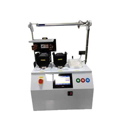
Semiconductor microscopes are essential tools in the semiconductor industry, enabling engineers and researchers to examine and analyze semiconductor materials and devices at a microscopic level. As a semiconductor microscope supplier, I often get asked about how these microscopes work. In this blog post, I'll break down the working principles of semiconductor microscopes in a way that's easy to understand.
The Basics of Microscopy
Before we dive into the specifics of semiconductor microscopes, let's quickly go over the basics of microscopy. Microscopes work by magnifying small objects or specimens so that we can see details that are otherwise invisible to the naked eye. There are different types of microscopes, but the most common ones used in semiconductor applications are optical microscopes and electron microscopes.
Optical Microscopes
Optical microscopes use visible light to illuminate the specimen and a series of lenses to magnify the image. They are relatively simple and inexpensive, making them a popular choice for basic semiconductor inspection. The light source in an optical microscope can be either transmitted through the specimen (transmitted light microscopy) or reflected off the specimen (reflected light microscopy).
In semiconductor applications, reflected light microscopy is often used to examine the surface of semiconductor wafers. The light is focused onto the wafer surface, and the reflected light is collected by the objective lens and magnified to form an image. This allows us to see surface features such as scratches, defects, and patterns on the wafer.
Electron Microscopes
Electron microscopes, on the other hand, use a beam of electrons instead of light to image the specimen. They offer much higher resolution than optical microscopes, allowing us to see details at the nanometer scale. There are two main types of electron microscopes: scanning electron microscopes (SEM) and transmission electron microscopes (TEM).
- Scanning Electron Microscopes (SEM): SEMs work by scanning a focused beam of electrons across the surface of the specimen. As the electrons interact with the specimen, they produce secondary electrons, backscattered electrons, and other signals that are detected and used to create an image of the surface. SEMs are commonly used for semiconductor inspection because they can provide high-resolution images of the surface topography and composition.
- Transmission Electron Microscopes (TEM): TEMs work by passing a beam of electrons through a thin specimen. The electrons that pass through the specimen are then focused onto a detector to form an image. TEMs are used to examine the internal structure of semiconductor materials and devices at the atomic level.
How Semiconductor Microscopes Work
Now that we have a basic understanding of microscopy, let's take a closer look at how semiconductor microscopes work. Semiconductor microscopes are designed to meet the specific needs of the semiconductor industry, such as high-resolution imaging, precise measurement, and non-destructive testing.


Sample Preparation
The first step in using a semiconductor microscope is to prepare the sample. This typically involves cutting the semiconductor wafer into smaller pieces and mounting them on a sample holder. The sample may also need to be polished or etched to improve the surface quality and make it easier to image.
Illumination
Once the sample is prepared, it is placed on the microscope stage and illuminated. In optical microscopes, the illumination can be provided by a variety of light sources, such as halogen lamps, LED lights, or lasers. The type of illumination used depends on the specific application and the type of microscope.
In electron microscopes, the illumination is provided by an electron gun, which produces a beam of electrons. The electron beam is then focused onto the sample using a series of electromagnetic lenses.
Imaging
After the sample is illuminated, the microscope captures an image of the sample. In optical microscopes, the image is formed by the objective lens and projected onto the eyepiece or a camera. In electron microscopes, the image is formed by the interaction of the electron beam with the sample and detected by a detector.
The image can be viewed in real-time on a monitor or saved for later analysis. Many semiconductor microscopes also have software that allows for image processing and analysis, such as measuring the size and shape of features, counting particles, and analyzing the composition of the sample.
Analysis
Once the image is captured, it can be analyzed to extract information about the sample. This may involve measuring the size and shape of features, counting particles, analyzing the composition of the sample, or detecting defects. The analysis can be done manually or using automated software.
Applications of Semiconductor Microscopes
Semiconductor microscopes are used in a wide range of applications in the semiconductor industry, including:
- Wafer Inspection: Semiconductor microscopes are used to inspect semiconductor wafers for defects, such as scratches, cracks, and particles. This helps to ensure the quality of the wafers and prevent defects from affecting the performance of the final semiconductor devices.
- Device Characterization: Semiconductor microscopes are used to characterize semiconductor devices, such as transistors, diodes, and integrated circuits. This involves measuring the electrical and optical properties of the devices and analyzing their performance.
- Failure Analysis: Semiconductor microscopes are used to analyze semiconductor devices that have failed. This involves examining the device under a microscope to identify the cause of the failure, such as a short circuit, an open circuit, or a defect in the material.
- Research and Development: Semiconductor microscopes are used in research and development to study new semiconductor materials and devices. This involves examining the structure and properties of the materials and devices at the microscopic level to understand their behavior and develop new technologies.
Our Semiconductor Microscope Products
As a semiconductor microscope supplier, we offer a wide range of semiconductor microscope products to meet the needs of our customers. Our products include:
- Microscope-Based Photoelectrical Analysis System: This system is designed for the photoelectrical analysis of semiconductor materials and devices. It allows for the measurement of the electrical and optical properties of the materials and devices under different conditions.
- Automated Wafer Inspection Microscope: This microscope is designed for the automated inspection of semiconductor wafers. It can detect defects, such as scratches, cracks, and particles, with high accuracy and speed.
- 3D Optical Profiler: This profiler is designed for the 3D measurement of semiconductor surfaces. It can provide high-resolution 3D images of the surface topography and measure the height, roughness, and other surface parameters.
Contact Us for Purchasing
If you're interested in purchasing a semiconductor microscope or learning more about our products, please contact us. We have a team of experts who can help you choose the right microscope for your specific needs and provide you with technical support and training.
References
- 1. Principles of Microscopy, Microscopy Society of America
- 2. Electron Microscopy: Principles and Techniques for Biologists, John Wiley & Sons
- 3. Semiconductor Manufacturing Technology, McGraw-Hill Education