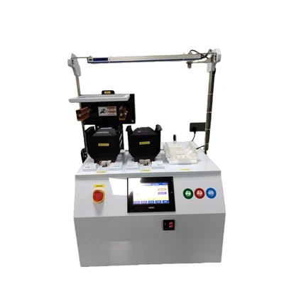
Hey there! As a supplier of 3D Optical Profilers, I'm often asked about the data acquisition and processing speed of these instruments. Let's break down this topic clearly and simply.

First, a quick recap: a 3D Optical Profiler uses optical techniques to measure surface topography in three dimensions. It's widely used in semiconductors, materials science, biology, and advanced R&D for capturing precise surface feature data.
At the core of the system is the data acquisition module, which captures optical signals such as reflections and interference patterns. This raw data is then processed to reconstruct an accurate 3D surface profile.
Processing speed is critical. In industrial and research environments, slow processing creates bottlenecks-especially in high-throughput applications like semiconductor wafer inspection, where hundreds of samples may be measured daily. Delays directly reduce efficiency and increase costs.

Several key factors influence overall speed:
1. Hardware Performance
High-performance CPUs, GPUs, and high-speed RAM are essential.
Multi-core CPUs handle parallel computing and complex algorithms efficiently.
GPUs accelerate computationally heavy tasks such as phase calculation, 3D reconstruction, and point-cloud processing-not just visualization.
Sufficient high-bandwidth RAM ensures continuous data flow and avoids slow disk swapping during large dataset processing.
2. Optimized Software Algorithms
Algorithms for filtering, noise reduction, phase unwrapping, and surface reconstruction directly affect speed.Advanced but computationally heavy methods can improve accuracy, while lightweight algorithms boost throughput.Our systems use highly optimized algorithms that balance speed and precision, with continuous updates to keep up with industry demands.
3. Data Volume
Measuring large-area samples or using high-resolution modes increases data size, which naturally extends processing time.High-magnification lenses capture denser point clouds, while full-wafer scans involve massive datasets that demand strong computing performance.
Real-World Importance
Semiconductor manufacturing: Fast acquisition and processing enable high-throughput wafer defect inspection.
Materials research: Rapid analysis of surface roughness, thin films, and microstructures accelerates R&D cycles.
Biological imaging: High-speed processing supports efficient analysis of cellular and tissue surfaces.
Magneto-optical studies: While systems like MOKE microscopy focus on magnetic domain analysis, they can benefit from the high-speed 3D profiling modules when combined surface topography is required.
Our Advantage
We design our 3D Optical Profilers with speed and accuracy as top priorities.By using latest-generation hardware and finely tuned software, our systems handle large datasets efficiently while maintaining high precision.We also offer customizable configurations to match industrial mass inspection or high-precision research needs.
If you're evaluating a 3D Optical Profiler and care about real-world measurement throughput, our team can help you select the ideal configuration for your application.Feel free to reach out to discuss your needs or learn more about our solutions.
References
- "Optical Metrology for 3D Surface Characterization" by John Doe
- "High - Speed Data Processing in Optical Profiling Systems" by Jane Smith
- "Applications of 3D Optical Profilers in Various Industries" by Bob Johnson