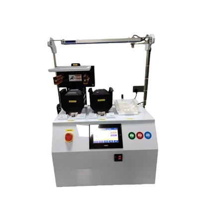
Product overview
The Ion Implantation System is a key piece of process equipment for semiconductor manufacturing and advanced material development. It is widely used in integrated circuit fabrication, compound semiconductor processing, and functional material modification. We have developed a full lineup of Ion Implantation Systems covering medium-current, high-current, high-energy, custom-configured, and compound semiconductor-specific models to meet diverse process requirements across different application scenarios.
Advantages
High ion beam purity: The system incorporates advanced ion source and beamline purification designs, which effectively suppress unwanted impurity ions. This ensures stable, high-quality implantation and supports consistent device performance in high-volume production.
Long ion source lifetime: Optimized ion source structure and material selection extend service intervals, reduce maintenance frequency, and lower overall operating costs for users.
Wide process window: The implanter supports a broad range of implantation energy and dose settings, making it suitable for shallow junction formation, deep buried layer doping, and other critical steps in advanced device manufacturing.
High production efficiency: Fast automatic beam tuning reduces setup time and improves throughput. The stable, reliable operation helps maintain high utilization in continuous manufacturing environments.
Applications
Integrated circuits: Used for doping in transistor source/drain formation, threshold voltage adjustment, well and isolation implants, and other core steps in logic, memory, and analog chip manufacturing.
Compound semiconductors: Applied to doping and modification of GaAs, GaN, and other compound materials, supporting the production of RF devices, optoelectronic chips, and power semiconductors.
Advanced materials: Used for surface doping, property modification, and structural adjustment of metals, ceramics, and new functional materials, enabling improved electrical, optical, and mechanical performance in research and industrial applications.
Parameters
| Parameter Item | Specification |
|---|---|
| Energy Range | 2 - 900 keV |
| Wafer Size | 12 inch, 8 inch |
| Energy Accuracy | ±1% |
| Tilt Angle Control Range | 0 - 45° |
| Angle Accuracy | ±0.1° |
| Ion Source Lifetime (Gas Source) | ≥700 h |
| Ion Source Lifetime (Solid Source) | ≥50 h |
| Max Beam Current (12 inch, B+) | 2500 μA |
| Max Beam Current (12 inch, As+) | 1300 μA |
| Max Beam Current (12 inch, P+) | 2500 μA |
| Max Beam Current (8 inch, B+) | 2000 μA |
| Max Beam Current (8 inch, As+) | 1300 μA |
| Max Beam Current (8 inch, P+) | 2000 μA |
| Dose Uniformity (1σ) | ≤0.5% |
| Dose Repeatability (1σ) | ≤0.5% |
| Dose Range | 2E11 - 1E16 ions/cm² |
| Mechanical Transmission Efficiency | 380 pieces/h |
| Fragmentation Rate | 1:100000 |
| Applications | LOGIC, DRAM, 3D NAND, NOR, CMOS, MOSFET, IGBT, BCD, CIS, DMEMS, etc. |
FAQ
Q: What is an Ion Implantation System?
A: An Ion Implantation System is a key semiconductor equipment used for doping wafers by implanting ion beams, widely used in integrated circuits and compound semiconductor manufacturing.
Q: What are the main advantages of your Ion Implantation System?
A: Our Ion Implantation System features high ion beam purity, long ion source lifetime, wide energy/dose ranges, fast automatic beam tuning, and high production efficiency.
Q: What applications does the Ion Implantation System support?
A: It supports integrated circuit manufacturing, compound semiconductor processing, and advanced material modification for better electrical and optical performance.
Q:Can you provide customized Ion Implantation System solutions?
A: Yes, we offer customized models for medium-current, high-current, high-energy, and compound semiconductor-specific applications.
Q: How does high ion beam purity improve production?
A: High purity reduces impurities, stabilizes the implantation process, and improves device yield and reliability in mass production.
Hot Tags: ion implantation system, China ion implantation system manufacturers, suppliers