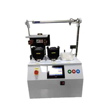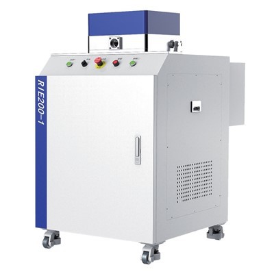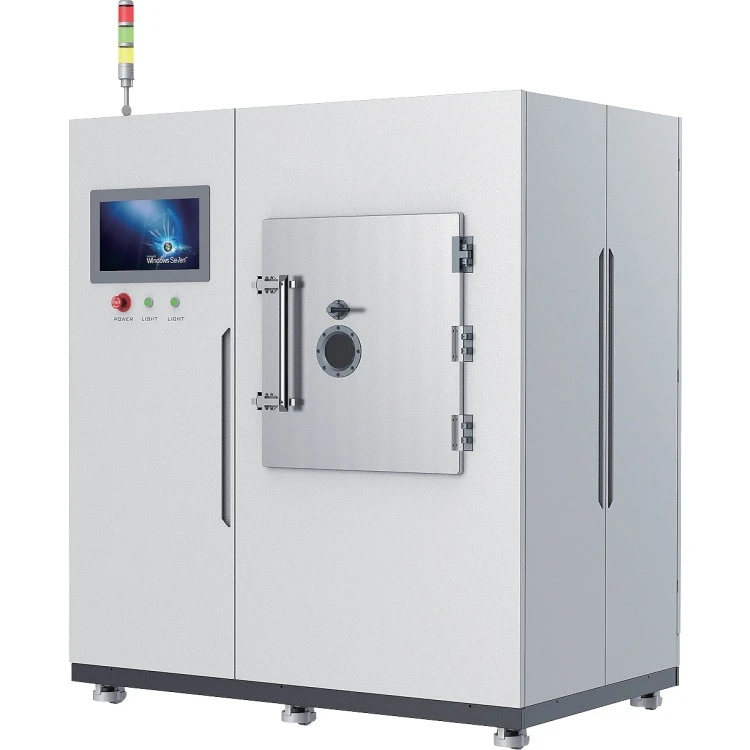
Product overview
Ion Beam Etching (IBE) machines are high-precision processing tools built around physical ion beam etching tech. The core idea? Blast material surfaces with high-energy ion beams to strip away atoms-perfect for non-destructive processing of tough-to-etch brittle materials (like metals and ceramics) and sensitive quantum chip materials.
They come with a dual-mode worktable: a single-piece one with angle adjustment from -90° to 90°, plus a multi-piece circular rotating type. Whether you're doing small-batch lab research or mass production, it flexes to fit your needs. There's also a water cooling/helium back cooling system to keep wafers from thermal damage-so precision devices like quantum chips stay stable after processing.
On top of that, ion beam energy adjusts smoothly from 0 to 1000 eV. Pair that with etching uniformity of ≤±3% (for 8-inch substrates), and you can nail precise control over etching depth and pattern accuracy. It's a core process workhorse for R&D on advanced semiconductors (silicon carbide, 2D materials), high-precision optoelectronic device manufacturing, and quantum chip development.
Applications
1. Hard-to-etch materials: Superconducting metals, ceramics (aerospace, high-end tools)
2. Quantum chips: Low-damage etching of qubits/quantum dots
3. Advanced semiconductors: SiC, GaN, 2D materials (R&D verification)
4. Optoelectronics: Optical communication devices (5G/6G compatible)
5. MEMS: High-aspect-ratio structures (automotive, aerospace)
Advantages
1. Low-damage & high-precision: Physical etching, atomic control (quantum chips)
2. Brittle material-friendly: Superconducting metals, ceramics, SiC (no tweaks)
3. Flexible worktable: Dual-mode (-90°~90°/rotation) – R&D/mass production
4. Solid thermal management: Water/helium cooling (no thermal damage)
5. Tunable & consistent: 0-1000 eV + ≤±3% uniformity (steady batches)
Parameters
|
Item |
Specific Indicators |
|
Applicable Substrate Size |
≤8 inch(8 inch and below); some configurations support |
|
lon Beam Energy |
0-1000 eV, supporting continuous adjustment(0-1000 eV, |
|
lon Beam Current |
≤±1000 mA(for RF ion source);≤±200 mA(for Kaufman |
|
Etching Uniformity |
≤±3%(based on 8-inch substrate);≤±5%(based on 6- |
|
Substrate Stage Cooling Method |
Water cooling/ Helium back cooling |
|
Worktable Mode |
Dual-mode(Single-piece type: angle adjustable from-90° |
|
Positioning Function |
Supports Notch-point positioning |
|
Applicable Materials |
Metals(superconducting Nb, Al, etc.), ceramics, silicon |
FAQ
What's the max substrate size this IBE handles?
Up to 8 inches-some setups also work with substrates up to 6 inches.
How adjustable is the ion beam energy?
0-1000 eV, with continuous adjustment support.
How many worktable modes are there?
Two modes: single-piece (angle adjusts -90° to 90°) and multi-piece (circular rotation).
How's the substrate stage cooled?
Water cooling/helium back cooling-keeps substrates safe from thermal damage during etching.
Can it process superconducting materials (like Nb, Al)?
Yep-also handles ceramics, SiC, 2D materials (MoS₂), and compound semiconductors.
What are the beam current ranges for different ion sources?
RF ion source: ≤±1000 mA; Kaufman ion source: ≤±200 mA.
What's the etching uniformity?
≤±3% for 8-inch substrates, ≤±5% for 6-inch (calculated as (Max - Min)/(2×Average)).
Does it support precise substrate positioning?
Sure-comes with Notch-point positioning to lock in processing accuracy.
Any adaptive designs for quantum chip processing?
Low-damage physical etching plus water/helium cooling-cuts thermal damage and preserves material properties, perfect for quantum chip sensitive structures.
Can it switch between small-batch R&D and mass production?
Absolutely-dual-mode worktable fits both: single-piece for small-batch multi-angle tests, multi-piece for mass production.
Hot Tags: ion beam etching equipment, China ion beam etching equipment manufacturers, suppliers, RIE System, Ion Beam Milling System, Ion Beam Etcher, HDP Etcher, Reactive Ion Etching System, ICP Dry Etcher