Product overview
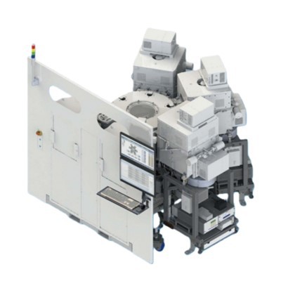
Our E-Beam Lithography System is a high-end piece of equipment made for creating micro- and nano-scale patterns-we use high-energy electron beams for direct writing here. By getting precise control over how the electron beam scans and exposes the sample surface, you can do maskless patterning with really high resolution. It's packed with advanced electron optics, real-time aberration correction, and multi-mode imaging too. All that makes it a go-to for R&D and fabrication in cutting-edge fields: semiconductors, photonics, quantum tech, you name it.
Advantages
1. Ultra-High Precision Patterning: It hits nanometer-scale resolution-more than enough to meet those tough fabrication demands you might have.
2. Maskless Direct Writing, Flexible and Efficient: No need for physical masks here. That means you can tweak designs in real time, cut down on development time a lot, and save on mask costs too.
3. Multi-Mode Imaging: Combines both Secondary Electron (SE) and Backscattered Electron (BSE) imaging. This lets you observe and align things in-situ while the exposure is happening-super handy for accuracy.
4. Intelligent Aberration Correction: Has automatic deflection aberration correction. This makes sure patterns stay uniform and accurate, even when exposing large areas.
5. High Process Compatibility: Works with a variety of materials and substrate types. Whether you're doing R&D or small-batch production, it fits the bill.
Applications
This system gets put to work across a bunch of key areas and processes, pretty extensively:
1. Compound Semiconductor Chips: We're talking fabrication of fine structures-like T-gates in HEMT devices, for example.
2. Quantum Chips: Patterning nano-scale components such as quantum dots and superconducting circuits; these are critical for quantum tech development.
3. Photonic Devices: Exposure work for optical gratings, metasurfaces, photonic crystals-all the structures that power photonic systems.
4. Advanced Electronic Devices: Supports patterning needs for low-dimensional materials and nano-devices, which are central to frontier research right now.
5. Semiconductor Mask Making: Capable of direct writing for high-precision photomasks, a key step in semiconductor manufacturing.
FAQ
Q: What is an E-Beam Lithography System?
A: A high-precision tool using electron beam direct writing for maskless, nanometer-scale patterning in micro/nano fabrication.
Q: What resolution does it provide?
A: It offers nanometer-scale resolution for ultra-high precision patterning.
Q: What are the main applications?
A: Widely used for semiconductor chips, quantum chips, photonic devices, nano-devices, and photomask fabrication.
Q: What are the key advantages?
A: Maskless direct writing, high flexibility, real-time design adjustment, low cost, and wide material compatibility.
Q: Does it support in-situ imaging?
A: Yes, with integrated SE/BSE imaging for real-time observation and alignment during exposure.
Hot Tags: e-beam lithography system, China e-beam lithography system manufacturers, suppliers, Coating and Developing System, Developer System, Maskless Lithography Machine, maskless uv lithography machine, Photoresist Coater and Developer, semiconductor lithography machine