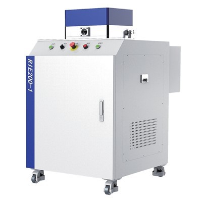
Product overview
The 6-inch CCP etching tool for small-to-medium production and R&D. Using CCP tech, its single chamber generates plasma to etch materials; volatile byproducts are removed via vacuum. It works with ≤6-inch wafers, offers flexible, cost-effective solutions for low-to-medium precision microstructures-ideal for both industry and labs.
Advantages
Super space-efficient
Its single-chamber build keeps the footprint tiny-perfect for cramped production lines or labs, and it'll slash your setup costs too.
Easy on the budget
We've refined the design and used tried-and-true components, so it delivers steady performance without breaking the bank.
Super versatile
It handles etching for Si, SiO₂, SiNₓ, Au, Ta-you name it. No matter what you're working on, it's got you covered.
Tailored process focus
It's great for photoresist descum and dielectric etching, with pinpoint parameter control to keep results consistent every time.
Applications
Micro-nano device making: It shapes microstructures for small semiconductor parts-perfect for components that need low-to-medium precision.
Descum & dielectric etching: Wipes out photoresist residue and etches dielectric materials, so your device surfaces stay clean and intact.
R&D and prototyping: Labs and enterprise R&D teams love it as a go-to tool-great for testing new materials, new structures, and building prototypes.
Small-batch runs: Perfect for making custom sensors or microelectronic modules in small quantities-it balances efficiency and cost like a pro.
Parameters
|
Category |
Details |
|
Wafer Compatibility |
Max. 6-inch (150mm) wafers; compatible with 4-inch/2-inch wafers via adaptive carriers |
|
Plasma Source Technology |
Capacitively Coupled Plasma (CCP); single-frequency RF power supply (13.56MHz) |
|
Supported Etch Materials |
Silicon (Si), silicon dioxide (SiO₂), silicon nitride (SiNₓ), gold (Au), tantalum (Ta), photoresist |
|
Key Process Performance |
- Etching uniformity: ≤7% (within-wafer, 6-inch)- Etch selectivity (Si vs SiO₂): ≥20:1- Photoresist descum efficiency: ≥95% residue removal |
|
RF Power Range |
0-500W (adjustable in 1W increments); power stability: ±1% |
|
Chamber Configuration |
Single etching chamber; stainless steel cavity with ceramic coating; integrated vacuum exhaust system |
|
Vacuum Performance |
Base pressure: ≤5×10⁻⁵ Pa; pumping speed: ≥300 L/s |
|
Gas Control System |
4-channel mass flow controller (MFC); flow range: 0-200 sccm per channel; supported gases: SF₆, O₂, CF₄, Ar, N₂ |
|
Temperature Control |
Chuck temperature: 20-80℃ (adjustable); temperature stability: ±0.5℃ |
|
Production & Reliability |
- Batch processing time: 3-10 min per wafer (varies by process)- Mean Time Between Failures (MTBF): ≥250 hours- Footprint: ≤1.2m × 0.8m (L×W) |
|
Control Interface |
Touchscreen HMI; PLC control system; support process recipe storage (up to 100 sets) |
FAQ
Q: What wafer sizes does the system support?
A: Max 6-inch; compatible with 4-inch/2-inch via carriers.
Q: Which materials can it etch?
A: Si, SiO₂, SiNₓ, Au, Ta, and photoresist.
Q: What core processes is it used for?
A: Photoresist descum and dielectric etching.
Q: What's the within-wafer etching uniformity?
A: ≤7% (6-inch wafer).
Q: What's the system's footprint?
A: ≤1.2m × 0.8m (L×W), space-saving.
Hot Tags: 6" ccp etcher, China 6" ccp etcher manufacturers, suppliers, RIE System, Ion Beam Milling System, Ion Beam Etcher, HDP Etcher, Reactive Ion Etching System, ICP Dry Etcher