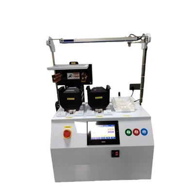
Hey there! As a supplier of 3D Optical Profilers, I often get asked if our 3D Optical Profiler can measure multi - layer structures. Well, let's dive right into it and find out.
First off, what exactly is a 3D Optical Profiler? It's a super - cool piece of tech that uses optical methods to measure the surface topography of an object in three dimensions. You can check out more about it 3D Optical Profiler. It can provide detailed information about the height, shape, and roughness of a surface. But when it comes to multi - layer structures, things get a bit more interesting.
Multi - layer structures are everywhere in modern technology. Think about semiconductor devices, where you have multiple thin layers of different materials stacked on top of each other. Each layer has its own properties and functions, and accurately measuring these layers is crucial for quality control, research, and development.
So, can our 3D Optical Profiler handle these multi - layer structures? The answer is a big yes! But there are some factors to consider.
One of the key aspects is the transparency of the layers. If the layers are transparent or semi - transparent to the light used by the profiler, the light can penetrate through the layers. The profiler can then detect the reflections from different interfaces between the layers. By analyzing these reflections, we can measure the thickness and topography of each layer.
For example, in a semiconductor device with multiple thin film layers, the 3D Optical Profiler can use interference patterns created by the reflected light. These patterns carry information about the distance between the interfaces of the layers, which allows us to calculate the layer thicknesses.
However, if the layers are opaque, the situation is a bit different. The light won't be able to pass through the opaque layer, and we'll only be able to measure the top surface of that layer. But in many cases, even with opaque layers, we can still get valuable information about the overall structure. We can measure the surface roughness, shape, and any defects on the top layer, which can be important for understanding the performance of the multi - layer structure.
Another factor is the refractive index of the materials in the layers. Different materials have different refractive indices, which affect how the light propagates through the layers. Our 3D Optical Profiler is designed to take these refractive index differences into account. It uses advanced algorithms to analyze the light signals and correct for any distortions caused by the refractive index variations.
Let's talk about the advantages of using a 3D Optical Profiler for measuring multi - layer structures. One of the biggest advantages is its non - contact nature. Unlike some other measurement methods that may require physical contact with the sample, the 3D Optical Profiler uses light to measure the surface. This means there's no risk of damaging the delicate multi - layer structures during the measurement process.


It also offers high - resolution measurements. We can get detailed information about the surface features of the multi - layer structure, down to the nanometer scale in some cases. This high resolution is essential for detecting small defects, variations in layer thickness, and other important characteristics.
In addition, the 3D Optical Profiler is relatively fast. It can measure a large area of the sample in a short time, which is great for mass production quality control. You can quickly check multiple samples and ensure that they meet the required specifications.
Now, let's compare our 3D Optical Profiler with some other measurement techniques for multi - layer structures. There are methods like electron microscopy, which can also provide high - resolution images of multi - layer structures. But electron microscopy usually requires a vacuum environment, and it can be time - consuming to prepare the samples. Our 3D Optical Profiler, on the other hand, can be used in a normal laboratory or production environment without the need for special sample preparation.
Another technique is atomic force microscopy (AFM). AFM can provide very high - resolution surface topography information. However, it has a relatively small measurement area, and it can be slow when measuring large samples. Our 3D Optical Profiler can cover a larger area in a shorter time, making it more suitable for large - scale production and inspection.
In some applications, our 3D Optical Profiler can even work in combination with other systems. For instance, you might want to use it along with the Microscope - Based Photoelectrical Analysis System. This combination can provide not only the surface topography information but also the photoelectrical properties of the multi - layer structure. Similarly, the Magneto - Optic Kerr Effect Microscopy System can be paired with the 3D Optical Profiler to study the magnetic and topographical properties of the multi - layer samples.
In conclusion, our 3D Optical Profiler is a powerful tool for measuring multi - layer structures. Whether the layers are transparent or opaque, it can provide valuable information about the surface topography and layer thicknesses. Its non - contact, high - resolution, and fast measurement capabilities make it a great choice for a wide range of applications in research, development, and production.
If you're working on projects involving multi - layer structures and are looking for a reliable measurement solution, our 3D Optical Profiler could be just what you need. Don't hesitate to reach out to us for more information or to discuss your specific requirements. We're always here to help you find the best way to measure and analyze your multi - layer samples.
References
- Some research papers on optical metrology of multi - layer structures
- Manufacturer's documentation of the 3D Optical Profiler