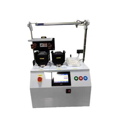
Environmental protection has become an increasingly crucial consideration in every industry, including the semiconductor microscopy sector. As a semiconductor microscope supplier, we recognize the significance of meeting environmental protection requirements not only for the health of our planet but also for the long - term sustainability of our business. In this blog, we will explore the key environmental protection requirements for semiconductor microscopes and how our products comply with these standards.


Energy Efficiency
One of the primary environmental concerns in the operation of semiconductor microscopes is energy consumption. High - energy microscopes can lead to increased electricity bills and higher carbon emissions. To address this issue, our semiconductor microscopes are designed with energy - efficient features.
We use advanced LED illumination systems instead of traditional halogen or mercury lamps. LED lights consume significantly less energy, have a longer lifespan, and do not contain harmful substances such as mercury. This not only reduces the energy usage of our microscopes but also minimizes the environmental impact associated with lamp disposal. For example, our Automated Wafer Inspection Microscope comes equipped with an energy - efficient LED lighting system that offers bright and uniform illumination while keeping energy consumption to a minimum.
In addition, our microscopes are designed with intelligent power management features. They can automatically enter a low - power standby mode when not in use, further reducing energy wastage. This ensures that the microscope consumes only the necessary amount of energy, even during periods of inactivity.
Material Selection and Recycling
The choice of materials in the manufacturing of semiconductor microscopes is another important aspect of environmental protection. We are committed to using sustainable and recyclable materials wherever possible.
For the exterior casings of our microscopes, we use high - quality plastics that are sourced from recycled materials or are easily recyclable at the end of the product's life. This reduces the demand for virgin plastics and minimizes the amount of plastic waste in landfills. The internal components are also designed for easy disassembly, which facilitates recycling at the end of the microscope's life cycle.
We also adhere to strict regulations regarding the use of hazardous materials. Our products are free from substances such as lead, mercury, cadmium, and brominated flame retardants (BFRs), which are restricted under the Restriction of Hazardous Substances (RoHS) directive. This ensures that our microscopes are safe for both the environment and the users.
Reducing Chemical Waste
Semiconductor microscopy often involves the use of various chemicals for sample preparation and cleaning. As a responsible supplier, we encourage our customers to use eco - friendly chemicals and provide guidelines on proper chemical handling and disposal.
We offer training programs and online resources to educate our customers on the safe and sustainable use of chemicals. For example, we recommend the use of water - based cleaning solutions instead of harsh solvents, which can be harmful to the environment and human health. Our 3D Optical Profiler is compatible with a wide range of eco - friendly cleaning agents, allowing users to perform high - quality inspections while minimizing chemical waste.
In addition, we work with our customers to develop waste management strategies for chemicals. We encourage the recycling and reuse of chemicals whenever possible to reduce the overall amount of chemical waste generated during the microscopy process.
Noise and Vibration Reduction
The operation of semiconductor microscopes can generate noise and vibrations, which can have a negative impact on the working environment. Our microscopes are engineered to minimize noise and vibrations.
We use advanced noise - cancelling technologies and vibration - dampening materials in the design of our products. This not only creates a more comfortable working environment for the users but also reduces the potential disturbance to the surrounding ecology. For example, our Magneto - Optic Kerr Effect Microscopy System is designed with a quiet and stable operation, ensuring that it can be used in noise - sensitive environments without causing disruptions.
Life - Cycle Assessment
To ensure that our semiconductor microscopes meet the highest environmental standards throughout their entire life cycle, we conduct comprehensive life - cycle assessments (LCAs). An LCA takes into account all the environmental impacts associated with a product, from raw material extraction and manufacturing to use and disposal.
By conducting LCAs, we can identify areas where we can further improve the environmental performance of our products. For example, we may find that a particular component in the microscope has a high environmental impact during the manufacturing process. In such cases, we can explore alternative materials or manufacturing processes to reduce the impact.
Compliance with International Standards
We are committed to complying with all relevant international environmental standards and regulations. Our products are certified to meet standards such as ISO 14001, which is an international standard for environmental management systems. This certification demonstrates our commitment to minimizing the environmental impact of our products and operations.
How Our Products Benefit the Environment
Our energy - efficient semiconductor microscopes can significantly reduce the carbon footprint of semiconductor manufacturing facilities. By using less energy, these facilities can save on electricity costs and contribute to a more sustainable future.
The use of recyclable materials and the reduction of hazardous substances in our microscopes also help to reduce the environmental impact associated with the disposal of electronic waste. This is in line with the global trend towards a circular economy, where resources are reused and recycled to minimize waste.
Contact Us for Sustainable Semiconductor Microscopy Solutions
As a leading semiconductor microscope supplier, we are dedicated to providing high - quality products that not only meet the technical requirements of our customers but also adhere to strict environmental protection standards. If you are interested in learning more about our semiconductor microscopes and how they can help you achieve your environmental and business goals, we invite you to contact us. Our team of experts is ready to assist you in selecting the right microscope for your specific needs and to provide you with detailed information on our environmental initiatives.
References
- ISO 14001: Environmental management systems - Requirements with guidance for use.
- Restriction of Hazardous Substances (RoHS) Directive.
- Various research papers on energy - efficient lighting and sustainable material use in electronics manufacturing.