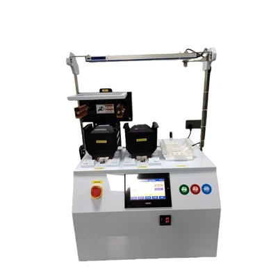
Ion beam etching (IBE) is a well - established technique in the field of microfabrication and surface engineering. As a supplier of Ion Beam Etching Equipment, I have witnessed firsthand the profound impact this technology has on surface modification. In this blog, we will explore the intricate relationship between ion beam etching and surface modification, delving into the principles, applications, and benefits of this synergy.
Principles of Ion Beam Etching
Ion beam etching is a physical process that uses a beam of energetic ions to remove material from a surface. In an IBE system IBE System, ions are generated in a plasma source, accelerated towards the target surface, and collide with the atoms of the target material. These high - energy collisions transfer momentum to the target atoms, causing them to be ejected from the surface in a process known as sputtering.
The energy and direction of the ion beam can be precisely controlled. By adjusting the ion energy, beam current, and angle of incidence, we can achieve different etching rates and profiles. For example, a higher ion energy generally leads to a faster etching rate, while a specific angle of incidence can be used to create anisotropic etch profiles, which are crucial for many microfabrication applications.
Surface Modification through Ion Beam Etching
Surface modification refers to the process of altering the properties of a material's surface to improve its performance in a specific application. Ion beam etching plays a significant role in surface modification in several ways.
1. Surface Cleaning and Preparation
One of the primary uses of ion beam etching is surface cleaning. Before any deposition or further processing, it is essential to have a clean and well - prepared surface. The energetic ions in the ion beam can remove contaminants such as oxides, organic residues, and adsorbed gases from the surface. This not only improves the adhesion of subsequently deposited films but also ensures the integrity of the surface for further processing steps.
2. Surface Roughness Control
Ion beam etching can be used to control the surface roughness of a material. By carefully selecting the etching parameters, we can either smooth or roughen the surface. For instance, low - energy ion bombardment can be used to smooth a rough surface by preferentially removing the high - points. On the other hand, high - energy ion etching can create a rough surface, which may be beneficial for applications such as improving the wettability of a surface or enhancing the optical properties.
3. Material Etching and Patterning
In the field of microfabrication, ion beam etching is widely used for material etching and patterning. By using a mask, we can selectively etch certain areas of the surface, creating micro - and nano - scale patterns. This is crucial for the manufacturing of semiconductor devices, microelectromechanical systems (MEMS), and optical components. For example, in the production of semiconductor chips, ion beam etching can be used to define the transistor gates and interconnects with high precision.
4. Interface Modification
Ion beam etching can also be used to modify the interface between two materials. When an ion beam is directed at the interface, it can cause intermixing of the atoms at the interface, which can change the chemical and physical properties of the interface. This can be beneficial for improving the adhesion between two materials or creating new functional interfaces.
Applications of Ion Beam Etching in Surface Modification
The combination of ion beam etching and surface modification has a wide range of applications in various industries.
1. Semiconductor Industry
In the semiconductor industry, ion beam etching is an essential process for the fabrication of integrated circuits. The high - precision etching capabilities of ion beam etching are used to create the complex structures and patterns required for modern semiconductor devices. For example, the 8" ICP Etcher is often used for etching silicon wafers to create transistors and other components with nanometer - scale features.
2. MEMS and NEMS
Microelectromechanical systems (MEMS) and nanoelectromechanical systems (NEMS) rely on ion beam etching for the fabrication of their tiny mechanical and electrical components. Ion beam etching allows for the precise control of the dimensions and shapes of these components, enabling the production of high - performance MEMS and NEMS devices such as accelerometers, gyroscopes, and resonators.
3. Optical Coatings
Ion beam etching is used in the production of optical coatings to improve the optical properties of the coatings. By controlling the surface roughness and the interface between the coating layers, ion beam etching can enhance the reflectivity, antireflectivity, and durability of the optical coatings. These coatings are widely used in lenses, mirrors, and optical filters.
4. Biomedical Applications
In the biomedical field, ion beam etching can be used to modify the surface properties of medical devices. For example, by creating a rough surface on an implant, ion beam etching can improve the cell adhesion and tissue integration of the implant, reducing the risk of rejection. It can also be used to etch micro - and nano - scale patterns on biosensors, enhancing their sensitivity and selectivity.
Benefits of Using Ion Beam Etching for Surface Modification
There are several benefits of using ion beam etching for surface modification compared to other surface treatment techniques.


1. High Precision
Ion beam etching offers high precision and control over the etching process. The ability to precisely control the ion energy, beam current, and angle of incidence allows for the creation of well - defined patterns and profiles with nanometer - scale accuracy. This level of precision is crucial for many high - tech applications such as semiconductor manufacturing and MEMS fabrication.
2. Anisotropic Etching
Ion beam etching can achieve anisotropic etching, which means that the etching rate is different in different directions. This is particularly useful for creating vertical or slanted sidewalls in microfabrication, which are difficult to achieve with other etching techniques. Anisotropic etching is essential for the production of high - aspect - ratio structures in semiconductor devices and MEMS.
3. Clean and Dry Process
Ion beam etching is a clean and dry process, which means that it does not involve the use of wet chemicals. This reduces the risk of chemical contamination and simplifies the post - processing steps. It is also more environmentally friendly compared to wet etching processes.
4. Compatibility with Different Materials
Ion beam etching can be used on a wide range of materials, including metals, semiconductors, insulators, and polymers. This makes it a versatile tool for surface modification in various industries. For example, the Metal Etching System is designed specifically for etching metal materials with high precision.
Contact for Procurement and Consultation
If you are interested in exploring the potential of ion beam etching for your surface modification needs, we are here to help. Our company specializes in providing high - quality Ion Beam Etching Equipment, including the 8" ICP Etcher, Metal Etching System, and IBE System. We have a team of experienced engineers who can offer technical support and consultation to ensure that you get the most suitable equipment for your specific applications.
Whether you are in the semiconductor industry, MEMS manufacturing, optical coating production, or biomedical field, our ion beam etching equipment can help you achieve the surface modification results you desire. Contact us today to start a discussion about your requirements and how our ion beam etching solutions can benefit your business.
References
[1] "Principles of Plasma Discharges and Materials Processing", by M. A. Lieberman and A. J. Lichtenberg.
[2] "Microfabrication Technology for Microelectromechanical Systems (MEMS)", by S. D. Senturia.
[3] "Ion - Beam - Assisted Deposition and Etching: Principles, Applications, and Future Trends" in Journal of Vacuum Science & Technology.