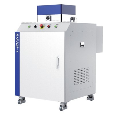
Product overview
This 8-inch ICP etching system is a mass-production-grade device for medium/small IC fabs and specialized processes. Featuring a high-stability ICP source, precision vacuum transfer, and closed-loop control, it enables ultra-precise etching of silicon, metals, and dielectrics. Compliant with 8-inch standards, it supports 0.11μm+ nodes and adapts to special semiconductor processing, balancing efficiency and flexibility for cost-effective solutions.
Advantages
Precise Control & High Yield
The self-optimized ICP source here really makes a difference-it ups plasma uniformity by 15%, with within-wafer uniformity ≤5% and wafer-to-wafer uniformity ≤3%. Then there's the 100:1 etching selectivity; that cuts down substrate damage a lot, and naturally, yield gets a nice boost too.
Robust Mass-Production & Cost-Saving
Let's get to the hard numbers-this system can handle 12,000 to 15,000 wafers per month. Reliability is solid too: MTBF is over 300 hours, and MTBC hits 350 RF-hours. Plus, its compact design saves 30% space, which in turn trims overall operating costs by 20%-that's a big win for budgets.
Broad Compatibility
It's pretty versatile when it comes to materials-silicon, Al/W metals, and SiO₂/Si₃N₄ dielectrics, all work with its etching process. And the modular interface is a lifesaver; switching parameters for logic, memory, or power semiconductors takes no time at all.
Intelligent Operation
The touch interface is user-friendly, and it comes with a built-in database and fault diagnosis tool. New operators? They can get up to speed in just a week. On top of that, real-time monitoring helps bring maintenance costs down-no more unnecessary expenses.
Applications
Mainstream 8-Inch IC Manufacturing: Core for 8-inch IC FEOL (gate, STI) and BEOL (Al wire, W plug) etching, fit 0.11μm-0.35μm logic/memory chips.
Specialized Devices: Custom recipes for IGBT/MOSFET electrode etching and LED/sensor patterning.
Capacity Upgrade: Expands mature 8-inch fab capacity; 6-inch compatible for flexible multi-size deployment.
R&D & Pilot Production: Essential for new material/process R&D in universities and enterprises, linking pilot and mass production.
Parameters
|
Category |
Details |
|
Wafer Compatibility |
8-inch (200mm) IC wafers; compatible with 6-inch wafers (optional) |
|
Supported Technology Nodes |
0.11μm – 0.35μm (mainstream nodes); adaptable to specialized processes |
|
Chamber Configuration |
High-stability ICP source + precision vacuum transfer module + descum chamber |
|
Etchable Materials |
Silicon, aluminum (Al), tungsten (W), silicon oxide (SiO₂), silicon nitride (Si₃N₄) |
|
Key Process Performance |
- Within-wafer uniformity: ≤5%- Wafer-to-wafer uniformity: ≤3%- Etch selectivity: Up to 100:1 |
|
Production Capacity |
12,000 – 15,000 wafers/month (standard process) |
|
Reliability Metrics |
- MTBF (Mean Time Between Failures): >300 hours- MTBC (Mean Time Between Cleans): 350 RF-h |
|
System Features |
Multi-parameter closed-loop control; modular process interface; intelligent fault diagnosis |
|
Space Requirement |
Compact design (30% space-saving compared to similar products) |
|
Operating Cost Advantage |
20% lower comprehensive operating cost than industry average |
FAQ
Q: What wafer sizes does the system support?
A: 8-inch (200mm) as standard; 6-inch compatible (optional).
Q: Which technology nodes are supported?
A: 0.11μm – 0.35μm mainstream nodes; adaptable to specialized processes.
Q: What materials can it etch?
A: Silicon, Al/W metals, SiO₂/Si₃N₄ dielectrics.
Q: What's the monthly production capacity?
A: 12,000 – 15,000 wafers (standard process).
Q: What are the key reliability metrics?
A: MTBF>300h; MTBC=350 RF-h.
Hot Tags: 8" icp etcher, China 8" icp etcher manufacturers, suppliers, RIE System, Ion Beam Milling System, Ion Beam Etcher, HDP Etcher, Reactive Ion Etching System, ICP Dry Etcher