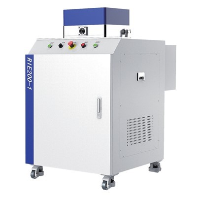
Product overview
This 8-inch ICP-DSE system is a mass-production etcher for high-aspect-ratio silicon processing. It integrates dual-frequency ICP power (2MHz+13.56MHz), our patented rapid gas switching module, and in-situ laser endpoint detection-with optimized Bosch alternating etching. Compliant with 8-inch wafer standards, it works with SOI, doped silicon, and SiC, enabling 10μm-1000μm precise etching. It balances R&D flexibility and mass-production stability, used in automotive sensors, super-junction MOSFETs, and TSVs.
Advantages
Excellent aspect ratio & profile control
100:1 ratio (10μm aperture, 1000μm depth) via improved Bosch process, with 90°±0.1° sidewall verticality, Ra 0.3μm roughness, and no "micro-trenches."
High mass-production efficiency
Up to 50μm/min etching rate (30+ wafers/hour per chamber). 3-chamber parallel design delivers 400 RF-h MTBC and 40% higher utilization. <1.0min gas switching and ±2% wafer-to-wafer error ensure batch consistency.
Low damage & high precision
Dual-frequency power offers >100:1 selectivity (vs SiO₂); 1μm laser endpoint accuracy, perfect for ultra-thin substrate TSV etching.
Wide adaptability
8-inch platform (6-inch compatible via carrier) with fast/slow Bosch mode. Supports Ar/O₂/C₄F₈/SF₆ for MEMS/power device processes.
Applicatios
MEMS: Deep trench/cavity etching for inertial/pressure sensors; automotive-grade verified.
Power Semiconductors: 100:1 aspect ratio etching for super-junction MOSFET/IGBT; used in high-reliability automotive/industrial devices.
Advanced Packaging: TSV etching for 8-inch WLP; laser detection ensures via depth uniformity for 3D stacking.
Special R&D: Etching for quantum chip silicon structures and inkjet printheads; one-click recipe storage for new materials.
Parameters
|
Category |
Details |
|
Wafer Compatibility |
8-inch (200mm) IC wafers; downward compatible with 6-inch wafers (via carrier) |
|
Supported Substrates |
Monocrystalline silicon, SOI (Silicon-On-Insulator), doped silicon, SiC (Silicon Carbide) |
|
Etching Depth Range |
10μm – 1000μm |
|
Key Process Performance |
- Aspect ratio: Up to 100:1- Sidewall verticality: 90°±0.1°- Sidewall roughness: ≤Ra 0.3μm- Wafer-to-wafer depth error: ±2% (mass production) |
|
Etching Rate |
Up to 50μm/min (silicon, standard Bosch process) |
|
Etch Selectivity |
>100:1 (silicon vs SiO₂ hard mask) |
|
Core Configuration |
Dual-frequency ICP power supply (2MHz + 13.56MHz); patented rapid gas switching module; in-situ laser endpoint detection system; helium backside cooling unit |
|
Production Capacity |
>30 wafers/hour per chamber (standard process); 3-chamber parallel design optional |
|
Reliability Metrics |
MTBC (Mean Time Between Cleans): 400 RF-h; Gas switching time: <1.0min |
|
Compatible Gases |
Ar, O₂, C₄F₈, SF₆, N₂ (supports multi-gas combination for customized processes) |
|
Endpoint Detection Accuracy |
1μm (laser in-situ detection) |
FAQ
Q: What wafer sizes does the system support?
A: 8-inch (200mm) as standard; 6-inch compatible via carrier.
Q: What's its maximum aspect ratio and etching rate?
A: Up to 100:1 aspect ratio; 50μm/min maximum etching rate.
Q: Which key devices can it serve?
A: Automotive-grade sensors, super-junction MOSFETs, IGBTs, TSVs, etc.
Q: What's the laser endpoint detection accuracy?
A: 1μm, ensuring precise etching depth control.
Q: What gases does it support?
A: Ar, O₂, C₄F₈, SF₆, N₂, and multi-gas combinations.
Hot Tags: icp deep si etcher, China icp deep si etcher manufacturers, suppliers, RIE System, Ion Beam Milling System, Ion Beam Etcher, HDP Etcher, Reactive Ion Etching System, ICP Dry Etcher