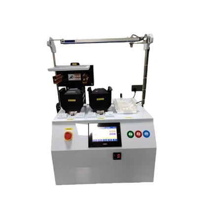
Ion Beam Etching (IBE) equipment is a cornerstone in the semiconductor and microfabrication industries, enabling precise material removal at the micro - and nanoscale. As a provider of Ion Beam Etching Equipment, I've witnessed firsthand the crucial role this technology plays in manufacturing high - precision components. However, ion beam contamination is a significant concern that can have far - reaching impacts on the etching process.
Understanding Ion Beam Etching
Before delving into the impact of contamination, it's essential to understand the basic principles of ion beam etching. In an IBE system, ions are accelerated towards a target material. These ions collide with the surface atoms of the target, causing them to be sputtered away. This process allows for highly accurate material removal, making it ideal for applications such as microelectromechanical systems (MEMS), integrated circuits, and optical device fabrication.
Sources of Ion Beam Contamination
Ion beam contamination can originate from multiple sources. One common source is the residual gas within the vacuum chamber of the IBE equipment. Even when the chamber is pumped down to a high vacuum, there are still trace amounts of gases such as oxygen, nitrogen, and hydrocarbons. These gases can interact with the ion beam and the target material, leading to unwanted chemical reactions.

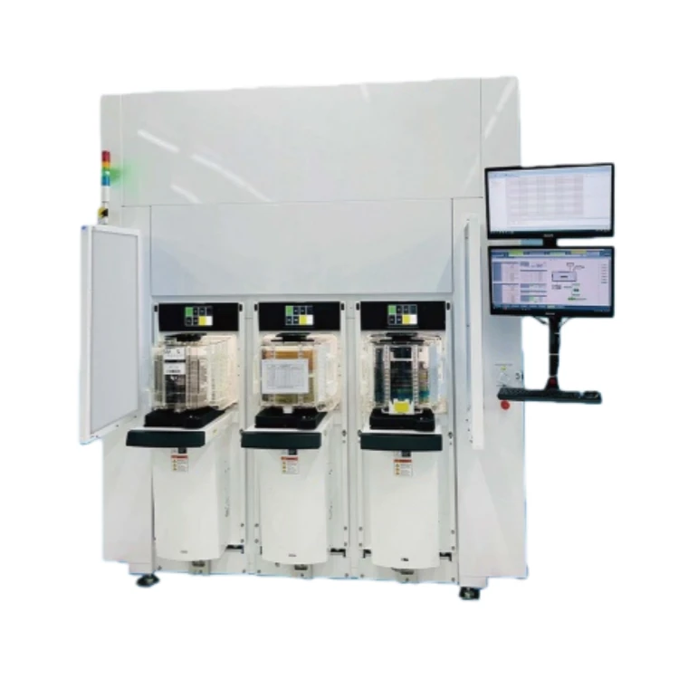
Another source of contamination is the ion source itself. Over time, the components of the ion source, such as the filament or the extraction electrodes, can degrade and release particles into the ion beam. Additionally, if the ion source is not properly maintained or calibrated, it may introduce impurities into the beam.
Impact on Etching Rate and Uniformity
One of the most significant impacts of ion beam contamination is on the etching rate. Contaminants can react with the target material, forming compounds that have different etching properties than the original material. For example, if oxygen is present in the ion beam, it can react with a metal target to form metal oxides. These oxides may have a lower etching rate than the pure metal, leading to a decrease in the overall etching rate.
Moreover, contamination can also affect the etching uniformity. Uneven distribution of contaminants across the target surface can result in non - uniform etching. Some areas may etch faster than others, leading to surface roughness and irregularities. This is particularly problematic in applications where high - precision and smooth surfaces are required, such as in the fabrication of optical lenses or micro - sensors.
Impact on Material Selectivity
Material selectivity is a critical aspect of the etching process. It refers to the ability to etch one material preferentially over another. Ion beam contamination can significantly reduce material selectivity. For instance, if a hard mask is used to protect certain areas of the target during etching, contaminants can react with the mask material, causing it to etch at a faster rate than expected. This can lead to under - etching or over - etching of the underlying material, compromising the integrity of the pattern.
Impact on Surface Quality
The surface quality of the etched material is also affected by ion beam contamination. Contaminants can cause surface damage, such as pitting or roughening. This is because the chemical reactions between the contaminants and the target material can create localized stress points on the surface. These stress points can lead to the formation of micro - cracks or other defects, which can degrade the performance of the final product.
Mitigating the Impact of Ion Beam Contamination
To minimize the impact of ion beam contamination, several strategies can be employed. First, maintaining a high - quality vacuum in the etching chamber is crucial. This can be achieved by using high - performance vacuum pumps and regularly cleaning the chamber to remove any residual gases.
Second, proper maintenance of the ion source is essential. This includes regular replacement of worn - out components and calibration of the ion source to ensure stable and clean ion beam generation.
Third, using appropriate shielding and filtering techniques can help reduce the amount of contaminants reaching the target material. For example, a gas filter can be installed in the ion beam path to remove any unwanted particles or gases.
Our Ion Beam Etching Equipment Solutions
As an Ion Beam Etching Equipment supplier, we offer a range of advanced systems designed to minimize the impact of ion beam contamination. Our Hard Metal - layer Etching System is specifically engineered for etching hard metal layers with high precision and minimal contamination. It features a state - of - the - art vacuum system and advanced ion source technology to ensure a clean and stable ion beam.
Our Hard Mask Etching System is optimized for applications where high material selectivity is required. It uses advanced shielding and filtering techniques to protect the hard mask from contamination, ensuring accurate pattern transfer.
In addition, our Silicon Etching System is designed to provide smooth and uniform etching of silicon materials. It incorporates advanced process control features to minimize the impact of contamination on the etching process.
Conclusion
Ion beam contamination is a significant challenge in the Ion Beam Etching process. It can have a profound impact on the etching rate, uniformity, material selectivity, and surface quality. However, with proper understanding and the use of advanced equipment and techniques, the impact of contamination can be effectively mitigated.
If you are in the market for high - quality Ion Beam Etching Equipment, we invite you to contact us for a detailed discussion. Our team of experts is ready to help you find the best solution for your specific needs.
References
- Smith, J. (2018). Ion Beam Etching Technology: Principles and Applications. Springer.
- Johnson, A. (2020). Contamination Control in Semiconductor Manufacturing. Wiley.
- Brown, C. (2019). Advanced Etching Processes for Microfabrication. Elsevier.